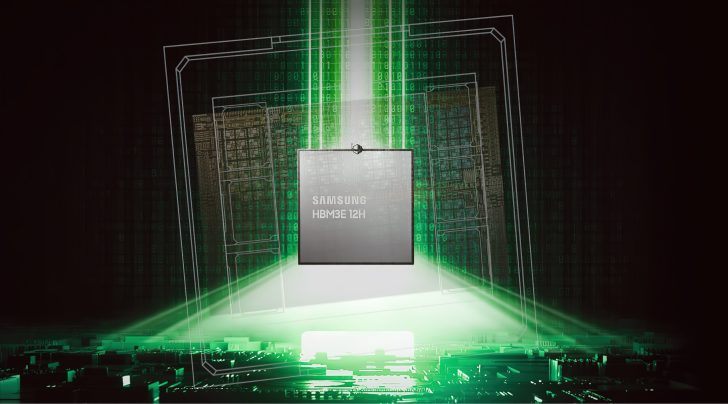
Samsung Passes NVIDIA‘s Test, HBM3E Mass Production is Ready
Samsung's HBM3E has passed NVIDIA's certification tests and is now in mass production, with shipments set to begin next quarter.
According to Korean media reports, Samsung Electronics' HBM3E memory has finally achieved its goal after several quarters - successfully passing NVIDIA's certification tests. Samsung has now commenced mass production of 8-layer HBM3E chips and is expected to start shipping next quarter. Concurrently, Micron Technology has also announced that it will supply HBM3E chips to NVIDIA.
HBM (High Bandwidth Memory) chips, with their superior memory bandwidth and efficiency, play a pivotal role in the current "AI era". They provide rapid access to large datasets and reduce latency, meeting the high computational demands of AI workloads such as deep learning and neural network training, significantly enhancing AI application performance.
Currently, NVIDIA holds approximately 80% of the global GPU market, especially in the AI application sector. Therefore, for HBM manufacturers, passing NVIDIA's tests is crucial not only for the company's reputation but also for driving profit growth.
For a long time, Samsung has been striving to obtain NVIDIA's certification for its HBM3E process to regain dominance in HBM technology and market share. To this end, Samsung has made several adjustments to its semiconductor business line, including forming a dedicated HBM team and reorganizing its DS (Device Solutions) division.
It is reported that Samsung has shifted its main production lines to HBM, allocating 30% of its existing DRAM capacity to HBM3E. This is estimated to reduce global DRAM supply by about 13%, causing an imbalance in DRAM supply and demand, potentially leading to price hikes. To address this subsequent issue, Samsung has converted its Pyeongtaek P4 plant into a production line dedicated solely to DRAM to ensure normal DRAM supply.
Industry insiders estimate that Samsung will announce this news at its financial report meeting at the end of the month. It is understood that Samsung's HBM3E memory technology uses its own 4nm process to manufacture logic chips, with the current yield rate exceeding 70%.

Earlier this year, it was reported that Samsung's HBM chips failed to pass NVIDIA's tests due to heat and power consumption issues, making them unsuitable for NVIDIA AI GPU accessories production. In contrast, Samsung's domestic competitor SK Hynix has been supplying HBM3E chips to NVIDIA since June 2022 and started supplying HBM3E chips to an undisclosed customer (believed to be NVIDIA) at the end of March this year.
As of today, the skyrocketing demand for NVIDIA's Blackwell products has significantly stimulated HBM demand. Samsung's production capacity far exceeds its competitors, giving it the opportunity to shine in this field. With the arrival of the next-generation Blackwell architecture, Samsung is poised to become an important partner for NVIDIA.
As of now, neither Samsung nor NVIDIA has commented on this.
·Original
Disclaimer: The views in this article are from the original Creator and do not represent the views or position of Hawk Insight. The content of the article is for reference, communication and learning only, and does not constitute investment advice. If it involves copyright issues, please contact us for deletion.