Samsung Refutes its 3nm Wafer Losses
There are rumours that Samsung foundry division in the semiconductor wafer production process of production defects, Samsung responded that the claim "no basis".
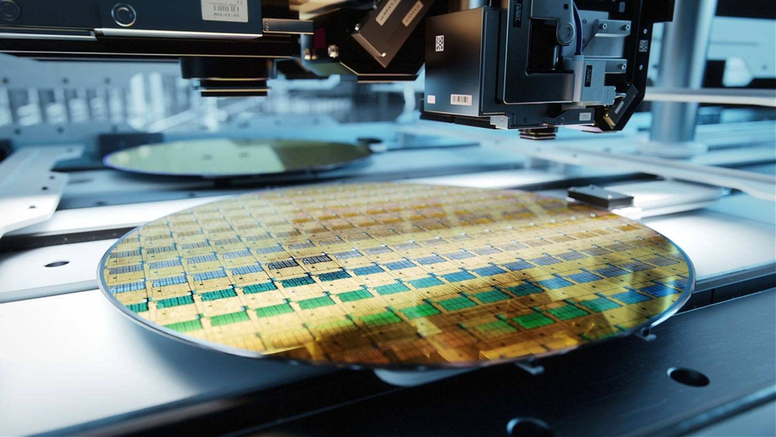
Recently, there have been rumors that Samsung Foundry has encountered production defects during the semiconductor wafer production process: in the second generation 3nm process, defects in 2,500 batches have resulted in a loss of ₩1 trillion (approximately $7.41 million), with each batch equivalent to producing about 65,000 12-inch wafers per month, all of which must be scrapped.
Media reports suggest that defects affecting quality occurred at Samsung Foundry, significantly impacting yield with damages estimated at around 500,000 wafers. Internally rated as a "Grade D incident," categorized as non-major within the company.
Shortly after, Samsung Electronics refuted these reports of "production defects," stating them "groundless." They argued that with a monthly production capacity of 60,000 chips and multiple inspection checkpoints in the production process, such large-scale defects are unlikely to occur.
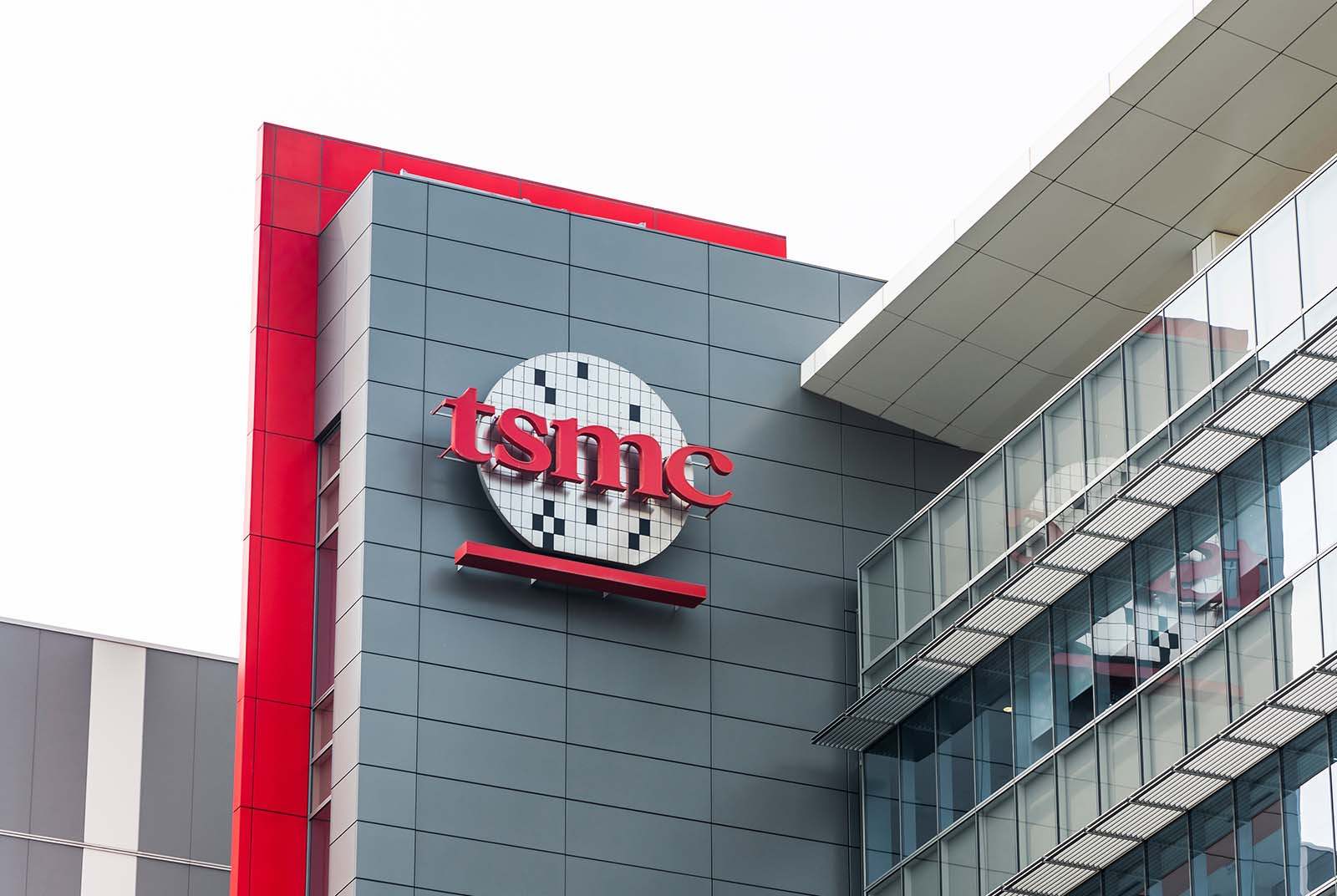
In chip manufacturing industry, Samsung stands as the world's largest semiconductor chip maker and the second-largest in the contract manufacturing sector.
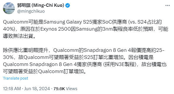
Recently, analyst Ming-Chi Kuo tweeted that Samsung's 3nm chip Exynos 2500 faced lower-than-expected yield rates, thus unable to ship. Consequently, Qualcomm will exclusively supply Samsung's Galaxy S25 series with its Snapdragon 8 Gen 4 chips manufactured by TSMC using the N3E process, with chip prices expected to rise by 25%-30%.
Currently, Samsung's Exynos 2500 chip yield rate remains below 20%, whereas mass production typically requires rates above 60%. Samsung's LSI division plans to achieve satisfactory yield rates for the Exynos 2500 chip by the second half of the year.
There are also reports suggesting that due to the uncertain mass production of the Exynos 2500 chip, Samsung is considering equipping the Galaxy S25 series with MediaTek's Dimensity chips to improve its negotiating position with Qualcomm.
However, with approximately 6 months left until the Samsung Galaxy S25 release, the outcome of these series' orders remains to be seen.
Recently, South Korean media reported that Samsung faced issues with yield rates and efficiency in its 3nm process, prompting major clients like Google and Qualcomm to transfer their orders to TSMC.
Looking back, Samsung's journey with 3nm technology actually began quite early. In 2017, Samsung announced the commencement of research and development for its 3nm process. By 2021, the 3nm node was successfully taped out, and by 2022, the 3nm GAA process entered mass production. Compared to TSMC, Samsung has maintained a lead of nearly six months.
Rough estimates suggest Samsung has invested approximately $116 billion in its entire 3nm project, excluding construction costs for two 3nm fabs in Arizona and Texas. However, the company's first-generation 3nm technology seems to have fallen short of expectations, with yield and power consumption control lagging behind TSMC by 10% to 20%.
In contrast, TSMC, leveraging its technological edge in the 3nm process, has attracted substantial orders from tech giants such as NVIDIA, AMD, Intel, Apple, Qualcomm, MediaTek, and Google. Customer orders are booked through 2026. The company reported that this year's 3nm production capacity has more than doubled compared to last year, yet it still falls short of customer demand. The goal is to quadruple capacity this year compared to last year.
According to industry analysts, the main reason major manufacturers are opting for TSMC lies in the different chip power efficiencies offered by the two companies in cutting-edge processes. Despite a 25% increase in production costs for 3nm chips, customers prioritize significant performance differences compared to the 5nm process.
On the other hand, the gap in market share between TSMC and Samsung's foundry businesses is widening. Data from market research firm TrendForce shows Samsung Foundry market share dipped slightly from 11.3% in the fourth quarter of last year to 11% in the first quarter of this year, while TSMC's market share during the same period rose from 61.2% to 61.7%.
Nevertheless, at its annual shareholders' meeting in March this year, Samsung expressed intentions to reclaim the top spot in the global chip market within the next two to three years.
Furthermore, Samsung has also unveiled its chip technology roadmap, which includes GAA (Gate-All-Around) processors designed with AI, to be implemented in the upcoming 2nm fabrication process.
Specifically, the second generation 3nm GAA is set to begin mass production in the latter half of this year; in 2025, Samsung plans to commence mass production of 2nm chips for the mobile sector; by 2026, expanding 2nm chip production to supercomputers and HPC chips; and by 2027, extending to automotive chips. Additionally, there are prospects for mass production of 1.4nm chips by 2027.
·Original
Disclaimer: The views in this article are from the original Creator and do not represent the views or position of Hawk Insight. The content of the article is for reference, communication and learning only, and does not constitute investment advice. If it involves copyright issues, please contact us for deletion.