SK Hynix, TSMC Teams Up: HBM Dominance Guaranteed
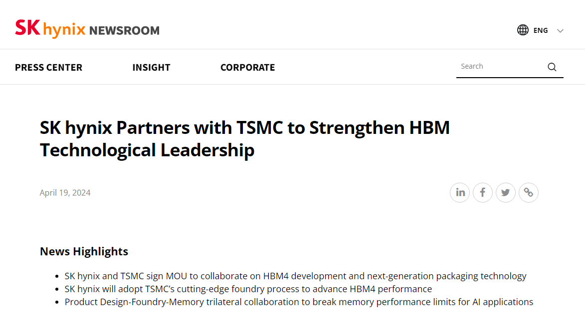
SK Hynix signs MOU with TSMC to enhance HBM4 performance using TSMC's cutting-edge foundry process and pioneer next-generation packaging technology. Breaking memory performance limits for AI applications through a three-way collaboration between product design, foundry and memory.
Recently, SK Hynix signs MOU with TSMC to enhance HBM4 performance. They aim to enhance the integration of logic and HBM through advanced packaging technologies, with mass production expected to commence in 2026.
SK Hynix has long dominated the HBM market and, alongside TSMC, serves as a top supplier for the American chip giant NVIDIA.
Since the launch of OpenAI's ChatGPT at the end of 2022, there has been a surge in demand for logic semiconductors (processors, storage chips), with NVIDIA taking the lead in the global AI revolution. Following suit, tech giants such as Apple, Microsoft, and Amazon have also joined the AI wave.
HBM, or High Bandwidth Memory, is a type of high-performance dynamic random-access memory (DRAM) based on 3D stacking technology. It is suitable for applications with high memory bandwidth requirements, such as GPUs, routers, and switches. Currently, HBM stands as the fastest DRAM product for data processing.
In 2013, SK Hynix first announced the success of HBM technology, with HBM1 making its debut in AMD's Radeon R9 Fury graphics card. This technology, which involves stacking memory chips and connecting them via through-silicon vias (TSVs), significantly improves memory bandwidth. Subsequently, HBM2, HBM2E, HBM3, and HBM3E have also been introduced in the HBM series.
Until HBM3E (the fifth generation), SK Hynix exclusively used its own process technology to produce HBM products. This technology, which involves stacking memory chips and connecting them via TSVs, significantly enhances memory bandwidth. Starting from HBM4 (the sixth generation), the company will adopt TSMC's advanced logic process technology, initially focusing on improving the performance of the base die within the HBM package.
Furthermore, both companies will optimize the integration of SK Hynix's HBM and TSMC's CoWoS (Chip-on-Wafer-on-Substrate) technology to jointly address customer demands for HBM in terms of performance and efficiency. CoWoS, TSMC's proprietary packaging technology, also known as "2.5D packaging," integrates logic chips and 3D HBM into a module, which is then mounted onto a 2D packaging substrate.
![]()
SK Hynix stated that the collaboration between the two companies will bring about richer technological innovations in the HBM field. Additionally, through product design, wafer fabrication, and memory tripartite cooperation, they aim to break the memory performance limitations in AI applications. In the future, AI semiconductors will transition from the era of 2.5D packaging in HBM to advanced packaging of 3D-stacked logic and memory chips.
Justin Kim, President and Head of AI Infra at SK Hynix, commented, "Through our partnership with TSMC, we can not only develop the highest-performance HBM4 but also actively expand open collaboration with global customers. In the future, the company will enhance the competitiveness of customized memory platforms for customers, further solidifying its market leadership position as a comprehensive supplier of AI memory."
Kevin Zhang, Senior Vice President of Business Development at TSMC, said, "Looking ahead to the new generation of HBM4, we believe that the two companies will continue to closely cooperate, providing the best inheritance solutions for our common customers and opening up new AI innovations."
According to publicly available market information, currently only SK Hynix, Micron Technology, and Samsung Electronics can provide HBM chips compatible with high-performance GPUs such as NVIDIA's H100.
Recently, Micron Technology also announced the start of production for its HBM3E chips, while Samsung released the industry's largest 36GB HBM3E 12H chip, which has been certified by NVIDIA.
According to Trendforce forecasts, SK Hynix is expected to occupy 52.2% of the global market share this year, followed closely by Samsung (42.4%) and Micron (5.1%). Additionally, the revenue share of HBM in the DRAM industry exceeded 8% in 2023 and is expected to reach 20% in 2024.
Allen Cheng, Director of the PwC Technology Industry Research Center, praised the collaboration between SK Hynix and TSMC. He believes that almost all major customers of TSMC are developing cutting-edge AI chips, and further deepening this partnership means that SK Hynix can attract more customers for its HBM products.
·Original
Disclaimer: The views in this article are from the original Creator and do not represent the views or position of Hawk Insight. The content of the article is for reference, communication and learning only, and does not constitute investment advice. If it involves copyright issues, please contact us for deletion.